Image


Renesas complementary product portfolios of Analog + Power + Embedded Processing + Connectivity work together to deliver comprehensive solutions.
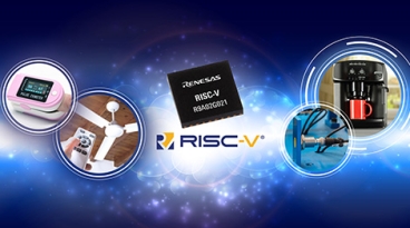
The industry’s first general purpose 32-bit RISC-V-based MCUs built with an internally developed CPU core let embedded system designers develop a range of power-conscious, cost-sensitive applications based on the open-source ISA and a full-scale development environment from Renesas and ecosystem partners.
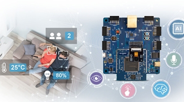
Complete reference solutions based on RA MCUs designed for easy integration of AI/ML technology feature Renesas and partner software for Real-time Analytics, Audio, and Vision applications.
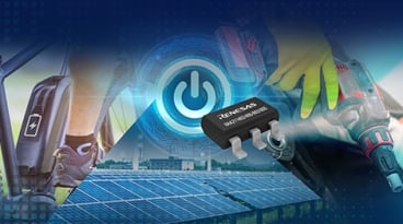
The RAA21140x and RAA21180x family of bucks are simple-to-use and cost-effective while offering more than 15x less power loss of similar output rating LDOs (depending on operating conditions) with ultra-low 4µA Iq at zero loading condition, making it idea.

JOIN US FOR AN EXCITING TECH DAY full of in-depth explorations into the benefits of
artificial intelligence, live showcases of cutting-edge AI applications, and expert dialogues.
Gain practical knowledge of Renesas’ newest AI-driven products and solutions, designed
to make our lives easier in the following topics:
-Cost-effective AI Solutions
-Emerging Wi-Fi Standards: Choosing the Best Path for Your Edge AI Needs
-How Arm® - Cortex®M85 Takes You Beyond M7 and Other High-performance MCUs
-MCU Real Time Analytics
-MPU Vision Artificial Intelligence
Visit demo stations and stay for our closing happy hour for your chance to win a set of Bose earbuds and other prizes!
Meals and refreshments will be served throughout the day.
JOIN US FOR AN EXCITING DAY full of technology deep-dives and leading-edge live demonstrations - focused on real showcases to get hands-on insights. Come meet our experts and:
- See how to practically enable AI/ML across a wide range of applications including industrial and automotive segments.
- Learn about pre-trained models ideally suited for AI/ML developers spanning across our embedded processing portfolio.
- Discover how to collect, analyze and optimize data ready to be deployed on tiny compute devices.
- Explore how our out-of-the-box tools and key technologies will kick-start your designs and turn your ideas on AI into real HW and SW.
- Play with our kits/tools and talk with our experts in front of leading-edge demos.
- Enjoy free food and drinks throughout the day, and have the chance to win an Apple Watch in our raffle.
Lectures and show and tell sessions are centered around Artificial Intelligence, Edge to Cloud and other key technologies.